


HITACHI 전자현미경
SU1510
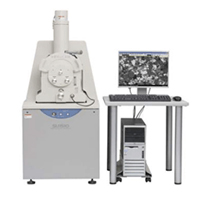
주요특징
- The footprint of the SU1510 has been reduced by 20% so that the microscope can be installed in more restricted places than before.
- To assist inexperienced users the SU1510 includes an on screen operation guide that walks the user step by step through the complete imaging process-from vacuum mode selection to taking a picture.
- Variable pressure mode for observation of non-conductive samples without the need for metal coating.
- High throughput, less floor space, less electric power consumption, with no cooling water requirement due to TMP evacuation system.
제품사양(Specification)
| (1) Resolution |
|---|
| SE : 3.0nm at 30kV (High Vacuum Mode) BSE : 4.0nm at 30kV (Low Vacuum Mode) |
| (2) Magnification |
| x5 to x300,000 (continuous) |
| (3) Accelerating voltage |
| 0.3 to 30kV |
| (4) Bias system |
| Quadrant bias system (HITACHI patent) |
| (5) Detectors |
| Everhart Thornley Secondary Electron Detector High sensitivity 5 segments BSE detector |
| (6) Low Vacuum Range |
| 6 to 270Pa through graphic menu |
| (7) Maximum loading sample size |
| 153mm dia. X 60mm H |
| (8) Image saving |
| Max. 5,120 x 3,840 pixels |
SU3500
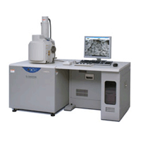
주요특징
- The SU3500 employs a new low-aberration objective lens and improved bias function that provides higher emission current at low kV. 7nm SE Image Resolution at 3kV, 10nm BSE Image resolution at 5kV.
- Unparalleled Image Quality : Novel and innovative electron optics and image display rendering engine
- Robustness & Versatility : Image observation and analysis without traditional specimen preparation techniques
- Intuitive Operation : Delegation technology affords easy operation and increased throughput efficiency
- Multi-Functional, Automated Specimen Stage : Enhanced navigation via new analytical chamber and automated stage functions
- The newly designed vacuum system enables low vacuum settings within the range of 6-650Pa
- The new Ultra Variable-pressure Detector(UVD)* is a highly sensitive detector for low vacuum mode, which is optimized for imaging surface details at low acceleration voltages.
- The new Live Stereoscopic function* provides real time 3D-SEM image without need for specimen tilting.
제품사양(Specification)
| (1) Resolution |
|---|
| SE : 3.0nm at 30kV (High Vacuum Mode) / 7nm at 3kV (High Vacuum Mode) BSE : 4.0nm at 30kV (Variable Pressure Mode) / 10.0nm at 5kV (High Vacuum Mode) |
| (2) Magnification |
| x5 to x300,000 (on photo) x7 to x800,000 (on display) |
| (3) Accelerating voltage |
| 0.3 to 30kV |
| (4) Bias system |
| Quadrant bias system (HITACHI patent) |
| (5) Detectors |
| Everhart Thornly Secondary Electron Detector High sensitivity semiconductor BSE detector |
| (6) Low Vacuum Range |
| 6 to 650Pa |
| (7) Maximum loading sample size |
| 200mm dia. x 70mm H (4-axis) 200mm dia. x 80mm H (5-axis) |
| (8) Image saving |
| Max. 5,120 x 3,840 pixels |
S-3700N
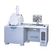
주요특징
- Large sample up to 300mm in diameter
- Observable area up to 203mm in diameter
- Observation and EDS analysis on a sample up to 110mm tall and 2kg weight
- EDS, EBSD and WDS simultaneously available
- Versatile port layout for various analytical applications
- 5-axis computer eucentric motorized stage with -20˚/+90˚ tilt
- One-button selectable High Vacuum/Low Vacuum Modes
- Ecological design by clean Turbo Molecular Pumping
제품사양(Specification)
| (1) Resolution |
|---|
| SE : 3.0nm at 30kV (High Vacuum Mode) / 10nm at 3kV (High Vacuum Mode) BSE : 4.0nm at 30kV (Low Vacuum Mode) |
| (2) Magnification |
| x5 to x300,000 (continuous) |
| (3) Accelerating voltage |
| 0.3 to 30kV |
| (4) Bias system |
| Quadrant bias system (HITACHI patent) |
| (5) Detectors |
| Everhart Thornley Secondary Electron Detector High sensitivity 5 segments BSE detector |
| (6) Low Vacuum Range |
| 6 to 270Pa through graphic menu |
| (7) Specimen stage |
| X : 150mm Y : 110mm Z : 5 to 65mm R : 360˚ T : -20˚ to +90˚ Maximum sample size : 300mm dia. X 110mm H |
| (8) Pumping system |
| TMP x 1 + R.P x 1 |
| (9) Image saving |
| Max. 5,120 x 3,840 pixels |